Electrical and mechanical failures are the most common failure modes encountered in Printed Circuit Boards (PCBs). Another not-so-obvious failure mode that can cause catastrophic failures in electronic products is the electrochemical failure mode, particularly the formation of the Conductive Anodic Filament (CAF). With the increase in electronic circuit density, the reduction in the pitch of vias has become inevitable which makes electronics vulnerable to CAF growth. CAF can cause short circuits and may pose serious threats to electronics reliability, especially in mission-critical applications. CAF is now becoming a common failure mode and a matter of concern for electronics manufacturers. Consequently, there is a great scope of research on CAF formation and the approaches to avoid it.
This article throws light on the formation of CAF and the factors responsible for their growth. To aid electronics manufacturers, the article discusses some potential ways to avoid CAF formation. Finally, some products from Chemtronics and Techspray are referenced that help inhibit the formation of CAF.
Conductive Anodic Filament (CAF) formation
CAF are metal filaments that originate from copper-plated vias along the fibers in PCB material i.e., the dielectric material. Their formation is due to the electrochemical migration in which conductive salt-containing copper forms in PCBs. The essential ingredients required for CAF formation include:
- Water – as an electrolyte
- Voltage gradient – as the driving force of the reaction
- Ions – as the electrical charge carriers
- Pathway – Passage for ions to move from one electrode (anode) to the other electrode (cathode)
Leftover solder flux also accelerates CAF formation. The starting point of CAF formation is the degradation of the glass/epoxy bond, which becomes the potential zone for moisture absorption. The degraded glass/epoxy interface later serves as an aqueous medium for the transport of electrochemical ions or corrosion products [1]. In this process, the copper traces serve as electrodes, water as an electrolyte, and voltage as the driving force. It is worth mentioning the reasons that lead to the degradation of glass/epoxy bonds. The most common reasons are thermal cycling and careless hole drilling. Both these events induce cracks between plated vias. As the plating solutions are highly ionic, they can ooze into the cracks forming a conductive residue between the anode and cathode. An important point to keep in mind is that CAF typically forms in the layers buried inside PCBs, as depicted in Figure 1.
How to identify CAF?
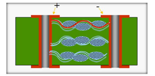 Figure 1: CAF formation between plated through hole vias [2]
To ensure the quality and reliability of electronic assemblies, the Institute of Printed Circuits (IPC) has developed a standard test procedure to measure CAF resistance. Specifically, it is known as the IPC-TM-650 method. This test utilizes standardized coupon designs including IPC-9253 to IPC-9256. The test coupons are powered up and exposed to high temperature (85oC) and high humidity (85% RH) conditions followed by insulation-resistance measurements. If the insulation resistance is degraded, the cause can be further identified using Scanning Electron Microscopy (SEM), X-Ray Photoelectron Spectroscopy (XPS), or the Focused Ion Beam (FIB). This microscopic characterization will confirm the presence of CAF in the PCB under test.
How to prevent CAF?
Ensuring the absence of any one of the four essential ingredients for CAF will prevent its growth. The following are strategies for preventing CAF:
- Avoid defects
- Ensure proper design
- Eliminate moisture
- Perform proper cleaning
Avoiding Defects
Any defect (e.g., crack, void or fracture) in PCB material may serve as a buried pathway for ions to move from the anode to the cathode. Drilling is the most likely cause of cracks in PCBs. Electronics manufacturers must pay close attention to drill bit size, drilling speed, drill press and drill feed rate to avoid defects in PCBs. If possible, laser drilling should be considered as an alternative to mechanical drilling.
If solder reflowing is to be done in an oven, care must be taken to prevent the board from thermal stresses as they can also cause mechanical damage to the PCB.
Proper Designing
The selection of PCB material is a key step in PCB design. Instead of traditional FR-4 materials, CAF-resistant materials are now preferred because of their superior thermal properties [3]. During manufacture of conventional epoxy, chlorine is a by-product which is essential for the formation of CAF. Therefore, in the design of CAF-resistant materials, chlorine is removed [3]. Materials with high resin content are also CAF-resistant materials.
It is important to maintain nominal clearance between the PCB conductors and PCB vias to avoid CAF formation. This is because the voltage gradient increases when conductors are closely placed.
Another good strategy to prevent CAF is to stagger the vias at an angle of 45 degrees [4].
Eliminating Moisture
Moisture enters PCBs by the process of condensation i.e., when the PCB surface is cooler than the surrounding air. Moisture is the root cause of most of the failure modes associated with electronics. Thus, the elimination of moisture from electronics is a key concern for electronics manufacturers. The Essential Guide To Waterproofing Electronics may provide some useful ideas for electronics manufacturers to prevent moisture ingress.
To remove moisture content from PCB, the general practice is to bake out the boards before starting the assembly process such that the IPC-1601 standard is met. Particularly, the FR-4 material is hygroscopic and it is preferable to bake out the FR-4 PCBs followed by vacuum sealing. The baking process involves heating the PCB at a temperature of 100oC and above (as per requirement). Care should be taken that the oven is clean and free from contamination. Moreover, the boards should be stacked vertically and parallel to each other in such a way that air can freely circulate around the boards. Baking the PCBs also helps prevent condensation, delamination, and outgassing [5]. To verify moisture elimination, boards are weighed before and after the baking process.
Proper Cleaning
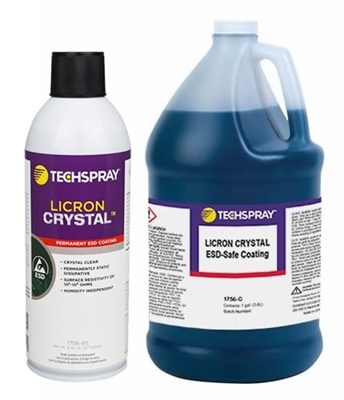
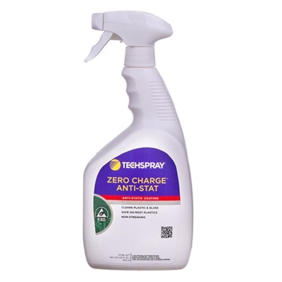
Contamination in the form of leftover flux residues serves as the ions (charge carriers) required for the process of electrochemical migration. It is therefore inevitable to clean the PCBs thoroughly before the application of conformal coating after the assembly process. The article on PCBA Cleaning & Conformal Coating Increase Reliability of Critical Systems may serve as a guideline for cleaning and selection of relevant products for electronics manufacturers. Techsprayhas been at the frontline of electronics maintenance and cleanliness since 1958. The extended line of flux removers offered by Chemtronics removes all types of no-clean, water-soluble, and synthetic flux.
For more information, contact your Techspray application specialist at 678-819-1408 or [email protected].
References
- C. Hu, "Study on the factors which affecting the conductive anodic filament reliability for packing substrate," in 2017 18th International Conference on Electronic Packaging Technology (ICEPT), Harbin, China, 2017.
- PreventLAB, "PreventLAB", 14-4-2017. [Online]. Available: http://blog.preventlab.eu/conductive-anodic-filament-failure-analysis-caf/. [Accessed 25-10-2022].
- A. Caputo, "Conductive Anodic Filament (CAF) Formation," University of Torronto, 2010.
- MCL, "Millennium Circuits Limited," Millennium Circuits Limited, [Online]. Available: https://www.mclpcb.com/blog/guide-pcb-caf-issues/. [Accessed 28-10-2022]
- >Henry, "The Engineering Knowledge," [Online]. Available: https://www.theengineeringknowledge.com/what-is-pcb-baking/. [Accessed 29-10-2022]
- C. Hu, "Study on the factors which affecting the conductive anodic filament reliability for packing substrate," in 2017 18th International Conference on Electronic Packaging Technology (ICEPT), Harbin, China, 2017.